- 您现在的位置:买卖IC网 > Sheet目录337 > LT1932ES6#TRMPBF (Linear Technology)IC LED DRIVR WHITE BCKLGT TSOT-6
�� �
�
�LT1932�
�PI� FU� CTIO� S�
�SW� (Pin� 1):� Switch� Pin.� This� is� the� collector� of� the� internal�
�NPN� power� switch.� Minimize� the� metal� trace� area� con-�
�nected� to� this� pin� to� minimize� EMI.�
�GND� (Pin� 2):� Ground� Pin.� Tie� this� pin� directly� to� local�
�ground� plane.�
�LED� (Pin� 3):� LED� Pin.� This� is� the� collector� of� the� internal�
�NPN� LED� switch.� Connect� the� cathode� of� the� bottom� LED�
�to� this� pin.�
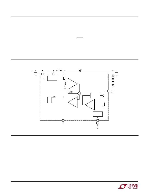
�BLOCK� DIAGRA�
�R� SET� (Pin� 4):� A� resistor� between� this� pin� and� ground�
�programs� the� LED� current� (that� flows� into� the� LED� pin).�
�This� pin� is� also� used� to� provide� LED� dimming.�
�SHDN� (Pin� 5):� Shutdown� Pin.� Tie� this� pin� higher� than�
�0.85V� to� turn� on� the� LT1932;� tie� below� 0.25V� to� turn� it� off.�
�V� IN� (Pin� 6):� Input� Supply� Pin.� Bypass� this� pin� with� a�
�capacitor� to� ground� as� close� to� the� device� as� possible.�
�V� IN�
�L1�
�D1�
�V� OUT�
�C1�
�5�
�SHDN�
�6�
�V� IN�
�1�
�SW�
�C2�
�DRIVER�
�Q1�
�+�
�0.04� ?�
�–�
�� 5�
�1.2MHz�
�OSCILLATOR�
�+�
�Σ�
�+�
�DRIVER�
�Q2�
�3�
�LED�
�I� LED�
�Q�
�S�
�+�
�R�
�A2�
�–�
�A1�
�–�
�+�
�LED� CURRENT�
�REFERENCE�
�2�
�GND�
�I� SET�
�4�
�R� SET�
�1932� F01�
�R� SET�
�Figure� 1.� LT1932� Block� Diagram�
�OPERATIO�
�The� LT1932� uses� a� constant� frequency,� current� mode�
�control� scheme� to� regulate� the� output� current,� I� LED� .�
�Operation� can� be� best� understood� by� referring� to� the�
�block� diagram� in� Figure� 1.� At� the� start� of� each� oscillator�
�cycle,� the� SR� latch� is� set,� turning� on� power� switch� Q1.� The�
�signal� at� the� noninverting� input� of� the� PWM� comparator�
�A2� is� proportional� to� the� switch� current,� summed� to-�
�gether� with� a� portion� of� the� oscillator� ramp.� When� this�
�signal� reaches� the� level� set� by� the� output� of� error� amplifier�
�A1,� comparator� A2� resets� the� latch� and� turns� off� the�
�power� switch.� In� this� manner,� A1� sets� the� correct� peak�
�current� level� to� keep� the� LED� current� in� regulation.� If� A1’s�
�output� increases,� more� current� is� delivered� to� the� output;�
�if� it� decreases,� less� current� is� delivered.� A1� senses� the�
�LED� current� in� switch� Q2� and� compares� it� to� the� current�
�reference,� which� is� programmed� using� resistor� R� SET� .� The�
�R� SET� pin� is� regulated� to� 100mV� and� the� output� current,�
�I� LED� ,� is� regulated� to� 225� ?� I� SET� .� Pulling� the� R� SET� pin� higher�
�than� 100mV� will� pull� down� the� output� of� A1,� turning� off�
�power� switch� Q1� and� LED� switch� Q2.�
�1932f�
�4�
�发布紧急采购,3分钟左右您将得到回复。
相关PDF资料
LT1937ES5#TRMPBF
IC LED DRIVR WHITE BCKLGT TSOT-5
LT3003EMSE#TRPBF
IC LED DRIVER BALLASTER 10-MSOP
LT3465AES6#TRMPBF
IC LED DRIVR WHITE BCKLGT TSOT-6
LT3466EDD-1#PBF
IC LED DRIVR WHITE BCKLGT 10-DFN
LT3466EDD#PBF
IC LED DRIVR WHITE BCKLGT 10-DFN
LT3474IFE#PBF
IC LED DRVR HP CONS CURR 16TSSOP
LT3475EFE-1#PBF
IC LED DRVR HP CONS CURR 20TSSOP
LT3476EUHF#PBF
IC LED DRVR HP CONST CURR 38-QFN
相关代理商/技术参数
LT1932ES6#TRMPBF (CUT REEL)
制造商:Linear Technology 功能描述:
LT1932ES6#TRPBF
功能描述:IC LED DRIVR WHITE BCKLGT TSOT-6 RoHS:是 类别:集成电路 (IC) >> PMIC - LED 驱动器 系列:- 标准包装:6,000 系列:- 恒定电流:- 恒定电压:- 拓扑:开路漏极,PWM 输出数:4 内部驱动器:是 类型 - 主要:LED 闪烁器 类型 - 次要:- 频率:400kHz 电源电压:2.3 V ~ 5.5 V 输出电压:- 安装类型:表面贴装 封装/外壳:8-VFDFN 裸露焊盘 供应商设备封装:8-HVSON 包装:带卷 (TR) 工作温度:-40°C ~ 85°C 其它名称:935286881118PCA9553TK/02-TPCA9553TK/02-T-ND
LT1932ES6TRMPBF
制造商:Linear Technology 功能描述:LED Driver 8-Seg 1.8/2.5/3.3/5/9V TSOT23
LT1933
制造商:LINER 制造商全称:Linear Technology 功能描述:1.4A, 500kHz Step-Down Switching Regulator
LT1933_1
制造商:LINER 制造商全称:Linear Technology 功能描述:600mA, 500kHz Step-Down Switching Regulator in SOT-23 and DFN Packages
LT1933ES6
制造商:Linear Technology 功能描述:Conv DC-DC Single Step Down 3.6V to 36V 6-Pin TSOT-23
LT1933ES6#PBF
制造商:Linear Technology 功能描述:IC STEP-DOWN REGULATOR 6-TSOT-23
LT1933ES6#TR
功能描述:IC REG BUCK ADJ 0.6A TSOT23-6 RoHS:否 类别:集成电路 (IC) >> PMIC - 稳压器 - DC DC 开关稳压器 系列:- 标准包装:2,500 系列:- 类型:升压(升压) 输出类型:可调式 输出数:1 输出电压:1.24 V ~ 30 V 输入电压:1.5 V ~ 12 V PWM 型:电流模式,混合 频率 - 开关:600kHz 电流 - 输出:500mA 同步整流器:无 工作温度:-40°C ~ 85°C 安装类型:表面贴装 封装/外壳:8-SOIC(0.154",3.90mm 宽) 包装:带卷 (TR) 供应商设备封装:8-SOIC